Fundamental Phenomena
COLLEGE OF NATURAL SCIENCES & MATHEMATICS
Students gain important experience at the cutting edge of two-dimensional matter.
The Nanoelectronics Group in the Department of Physics and Astronomy studies the properties of electrons traveling in single-layer materials—the closest that solid-state matter can get to two-dimensional. According to Associate Professor Dr. Claudia Ojeda-Aristizabal, “Nature always looks to minimize energy, to do things in the most effortless way. There are certain crystals in which the lowest-energy configuration is in two-dimensional layers.” Understanding these materials could lead to advances in quantum computing, solar energy, or flexible electronics, but scientists will not be able to gain full control of them for a long time. For now, the group is asking fundamental questions and observing, as Dr. Ojeda-Aristizabal says, “the beautiful phenomena that derive from the multiple constraints electrons find while traveling in these materials.”
Dr. Ojeda-Aristizabal’s experiments have been funded by the U.S. Department of Energy since 2017 with a $765,000 grant, which has allowed the study of multiple low-dimensional materials, from insulators to semiconducting molecules and metallic ferromagnets, providing training to various generations of masters and undergraduate students at CSULB. Her work also benefits from an $800,00 Partnership for Research and Education in Materials (PREM) grant from the National Science Foundation, which Dr. Michael Peterson sought and won for the department in 2022. The funding behind the Nanoelectronics Group mirrors its two defining characteristics: the pair of different methods that the group uses and the graduate and undergraduate students who have ownership of specific projects involving either method.

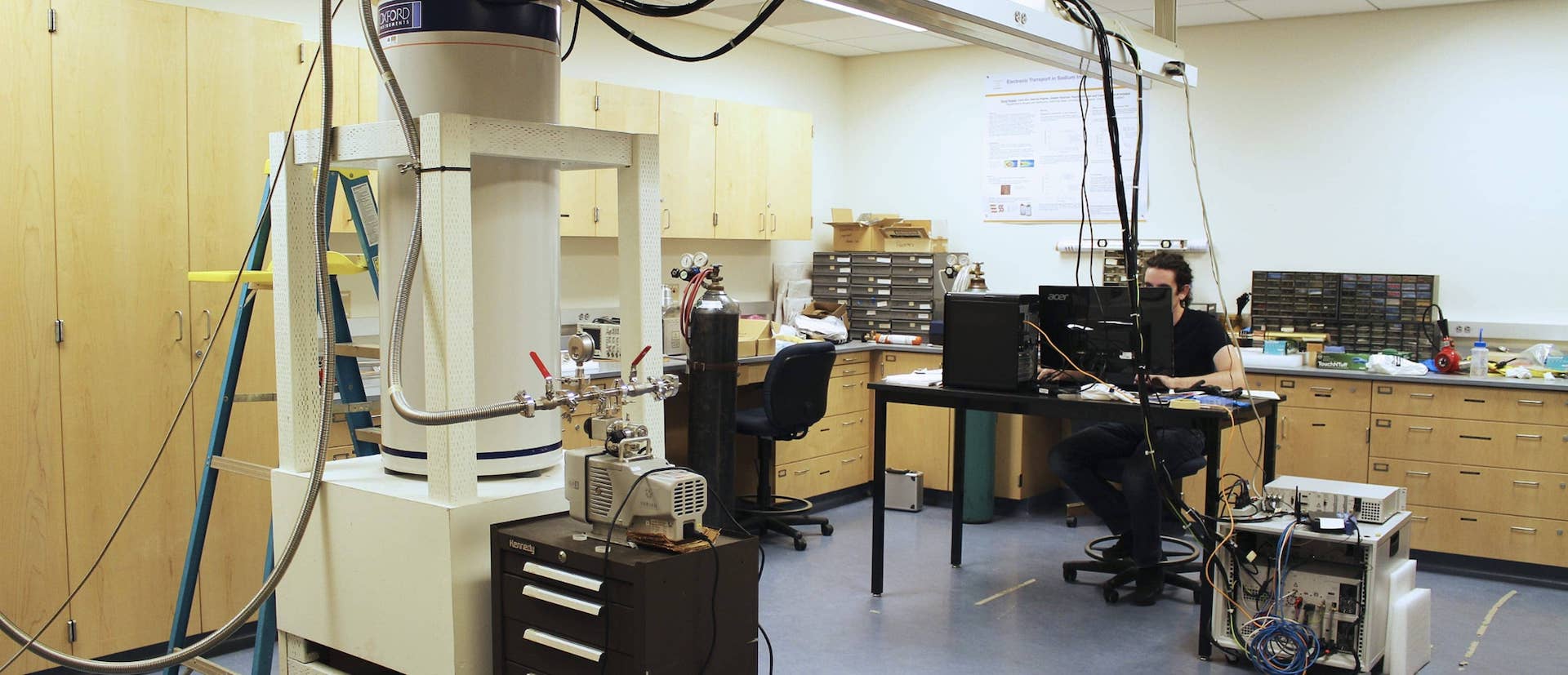
The first of the two research techniques, electron transport at low temperatures, takes place on campus at CSULB. Using this technique, simply put, students connect metallic electrodes to individual layers of the materials they are studying, run a current through the material, and measure the voltage drop across the electrodes at very low temperatures in the presence of a vertical magnetic field. The observations, after detailed analysis, give insight on the fundamental phenomena ruling the physics of the materials.
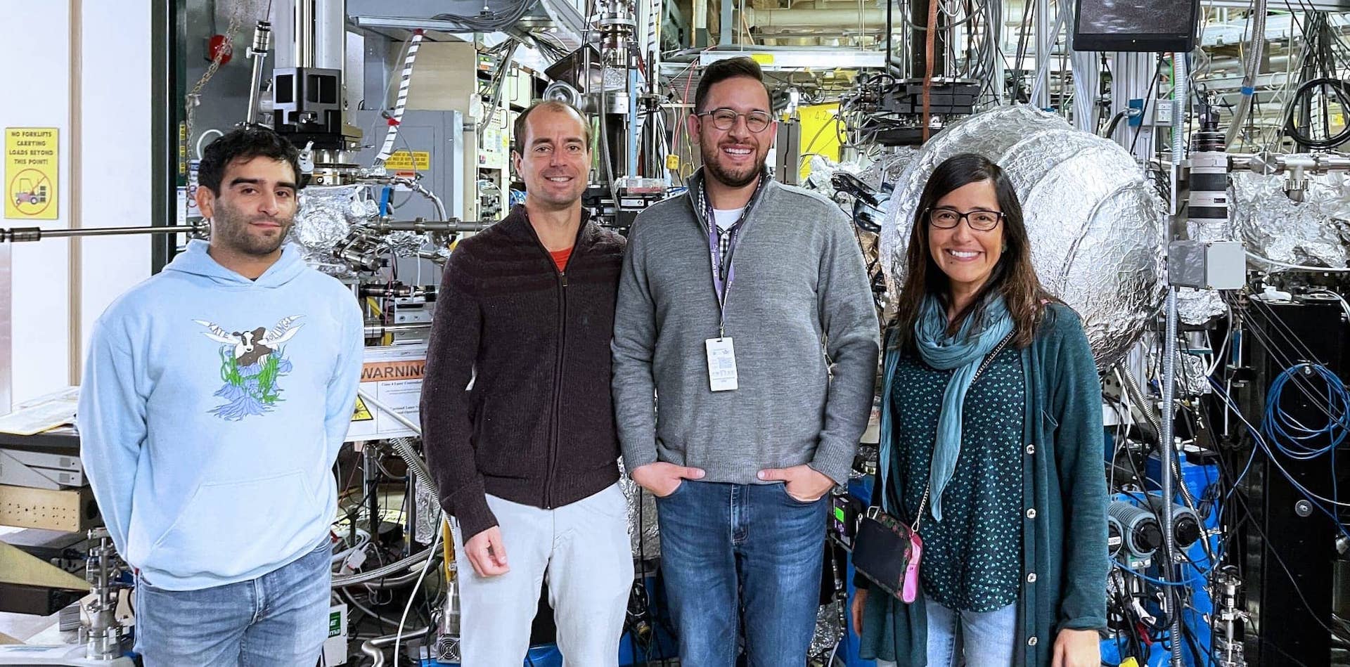
The second method, angle-resolved photoemission spectroscopy (ARPES), takes place at one of the best facilities in the world—the Lawrence Berkeley National Laboratory. In this technique, the energetic light of a synchrotron is shone into these materials, and the light excites photo electrons out. The excited photo electrons can be detected, together with their momentum and energy, which tells the scientists how the electrons are moving within the material. Dr. Ojeda-Aristizabal writes proposals to gain access to this laboratory, and her students are able to run experiments in the laboratory and interact with the scientists there at least twice each semester.
Both of these techniques contribute to findings in the group’s published papers, to which the students contribute directly. “It’s very neat that universities like Rice, Stanford, and Berkeley are confident in the abilities of students from CSULB,” says Dr. Ojeda-Aristizabal. Her students are, she says, “super motivated and not afraid to learn something new,” and though they may have followed an unconventional path to science, they are more resilient as a result.
Dr. Ojeda-Aristizabal says that she recently reminded a colleague at another institution that “I produce something that has more impact than papers; I produce successful students from Cal State.” While the effects of her laboratory experiments in tangible applications may not be known for decades, to the students learning how to perform those experiments, meaningful changes are happening now.